How are Solar Panels Made
#solarworld #solarPPA #commercialsolar #solarpanels #Trilectsolar
In recent years, solar panels have become more accessible than ever due to manufacturing efficiencies. Solar panels are now visible on the rooftops of many households and commercial properties.
But what are solar panels made of and how are solar panels made remains a mystery to many people contemplating installing solar panels to their home, business, farmlands or properties.
At Trilect Solar, we do not doubt that solar panels will be lighting up our neighbourhoods in the coming years. If you’re considering installing solar panels, you might be wondering “what are solar panels made of?”, and “how are solar panels made?”. Keep reading!
Silicon: The Raw Material
Silicon is the second most common element in the Earth’s crust. According to the Minerals Education Centre, silicon is not found in its pure form, but in compounds with Oxygen. Silica is one of the most abundant compounds which is found in rocks like obsidian, granite, and sandstone. Silicon can also be mined in quartzite, mica, and talc, but is found most abundantly in sand.
Silicon is reduced through a reduction process by heating it with carbon material to remove the Oxygen and leave behind a pure, metallurgical silicon. The silicon is purified into polysilicon which has a purity of over 99 percent.
Various grades of poly silicon can be created through different processes.
For example, electronic grade poly silicon, is extracted by passing poly silicon through hydrogen chloride at extremely high temperatures and then distilled.
To yield solar-grade silicon however, the poly silicon goes through a chemical refinement process. In the process, the silicon is passed through a mixture of gases to remove boron and phosphorus. The process results in pure cylindrical form solar grade silicon called ingots. The ingots are then sliced into small conductive pieces for photovoltaic panels.
Ingots to Wafers
The cylindrical ingots are cut into various wafers including monocrystalline, polycrystalline, and silicon ribbons. The main difference in the wafer quality is based upon the conducting efficiency of sunlight and the amount of energy wasted.
Monocrystalline wafers are thinly cut using a diamond saw into uniform crystals of silicon. The circular crystals are then cut into rectangular or hexagonal shapes to ensure a better fit. The process leads to a larger quantity of wasted silicon which can be recycled into poly silicon and recut.
Polycrystalline wafers are made from multiple crystal structures. The wafers are cut from cube-shaped ingots formed by pouring melted silicon into a cast. The structures produce less waste, but they are not as efficient as monocrystalline structures.
Silicon ribbons, better known as thin film, are made from multi crystalline silicon. They are so thing that they cannot be sliced into wafers. While the sheets are extremely thin and flexible, they are not as durable and require more support than other solar panel structures.
Wafer Doping Activation and the PN Junction
While the silicon wafers are ready, they cannot conduct any energy until they go through the doping process. This doping process involves the ionization of the wafer to create the p-n junction.
Silicon is a semiconductor, meaning it is neither a complete conductor, nor an insulator. This semiconductor material functionality makes it more efficient to convert the sunshine energy into electric energy. When Silicon absorbs light energy, or photons, it knocks out its electrons which then begin to move in the direction of the electric field creating a current. However, because Silicon is not a metallic element, the current produced is really small.
To overcome this matter, doping with small amounts of impurities can drastically increase the conductivity of the material. Usually semiconductors are doping using n-type (“N” for negative) and p-type (“P” for positive) dopants. N-type dopants act as electron donors as they have an extra valence electron which can be easily knocked out by a little bit of energy when incorporated into the atomic lattice of a semiconductor. P-type dopants assist in the conduction by accepting the electron knocked out of the n-type dopant.
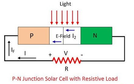
In the doping process, the wafers are heated at a very high temperature and put into water. The top layer of the cylinder is exposed to phosphorous, while the bottom layer is exposed to boron. The positive-negative junction is then created which allows for proper functioning.
After the doping process, the silicon is nearly ready to be processed into a functioning cell. However, due to the reflective characteristics of silicon, there is a considerable risk of losing potential solar energy. To minimize the reflective nature of the silicon wafers, the manufacturers coat the cell with silicon nitride, giving the cells the iconic blue look.
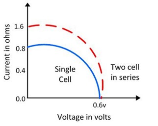
Series Combination of PV Cells
Attaching solar cells in a series combination means that the positive contact of one cell is connected to the negative contact of the second cell. This combination provides the same current as a single cell but doubles the voltage.
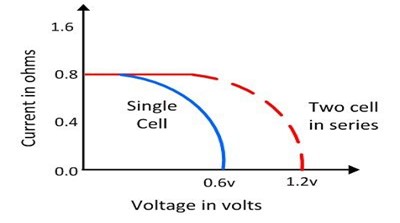
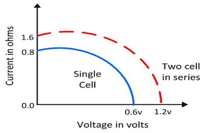
Parallel Combination of Solar Cells
Attaching solar cells in a series combination means that the positive contact of all cells are connected together, while the negative contact of all the cells are connected. This combination provides the same voltage as a single cell but double the current.
Series-Parallel Combination of PV cells
In a series-parallel combination, cells are connected in a matrix form creating a panel which produces a higher voltage and current producing capacity.
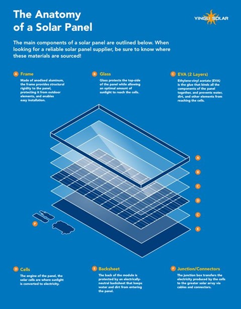
Assembling Cells into Solar Panels
A system is then implemented to collect and distribute the solar energy. This can be done by using a silicon screen or a screen-printing process in which a metal pathway is printed on both sides of the cell. These metal roadmaps provide the pathway for the energy to be collected, removed, and supplied to the receiver.
Solar panel manufacturers employ different proprietary processes to produce the final solar panel product. Usually, this is an automated process in which robots do the work. The cells are first put together to create a large sheet. According to some manufacturers, like Solar World, the process involves placing and soldering six strings of ten cells each, t make a rectangle of 60 cells. Each matrix is then laminated onto glass. The glass is then framed to make the panel sturdy and protect it from the weather it will endure. The electrical equipment that links the panel and receiver are then added.
Testing and Dispatch
Once the module is ready, various tests at STC (Standard Test Conditions) are carried out to ensure the solar panel performs as expected. The panel is put through a flash tester which delivers an equivalent of 1000 W/m2 of irradiance, 25OC temperature, and an air mass of 1.5g.
The panel is also tested in a more real-life scenario in which the panel faces 800 W/m2 of irradiance, 20OC temperature, and a wind speed of 1 m/s.
The electrical parameters and related ratings like power output, efficiency, voltage, current, and temperature tolerance are then noted into a technical sheet.
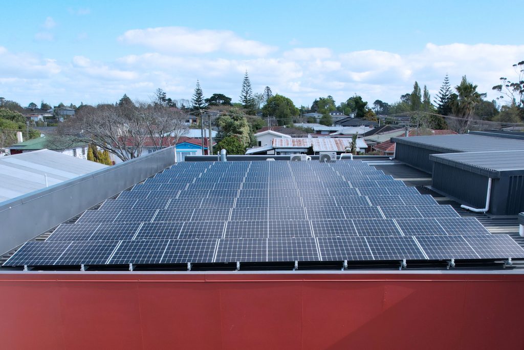
Once the modules clear the testing and inspection, the photovoltaic cells are ready for shipment to homes and business for installation.
References
https://greenerideal.com/guides/0613-solar-panel-basics-what-solar-panels-are-made-of/
https://courses.lumenlearning.com/introchem/chapter/doping-connectivity-of-semiconductors/#:~:text=In%20semiconductor%20production%2C%20the%20process,a%20deficiency%20in%20valence%20electrons.
Keywords: solar PPA, commercial solar, solar panels, Trilect Solar
ABOUT TRILECT SOLAR
Trilect Solar is a division of Trilect Services, New Zealand’s master electrician since 1997.
We are members of the Sustainable Energy Association of New Zealand (SEANZ) which offers additional peace of mind to our customers.
Trilect Electrical Services is a large electrical service company which is a member of the Master Electricians & Mastercraft network with 40 employees and a 20+ years history of customer satisfaction.
We do not use sub-contractors. All of the installations will be carried out by our experienced team.
Trilect Solar offers a customised energy plan that works for your home/ business.
Get started now by booking a free on-site consultation.
Request Your On-site Consultation
Or call us on 0800 850 888